- Overview
- Configuration
- NTP4 Plug-In
- Hardware
- RFC 868
- RFC 2030
-
RFC 1305
- RFC 1305
- 1. Introduction
- 1.1 Related Technology
- 2. System Architecture
- 2.1 Implementation Model
- 2.2 Network Configurations
- 3. Network Time Protocol
- 3.1 Data Formats
- 3.2 State Variables and Parameters
- 3.2.1 Common Variables
- 3.2.2 System Variables
- 3.2.3 Peer Variables
- 3.2.4 Packet Variables
- 3.2.5 Clock-Filter Variables
- 3.2.6 Authentication Variables
- 3.2.7 Parameters
- 3.3 Modes of Operation
- 3.4 Event Processing
- 3.4.1 Notation Conventions
- 3.4.2 Transmit Procedure
- 3.4.3 Receive Procedure
- 3.4.4 Packet Procedure
- 3.4.5 Clock-Update Procedure
- 3.4.6 Primary-Clock Procedure
- 3.4.7 Initialization Procedures
- 3.4.7.1 Initialization Procedure
- 3.4.7.2 Initialization-Instantiation Procedure
- 3.4.7.3 Receive-Instantiation Procedure
- 3.4.7.4 Primary Clock-Instantiation Procedure
- 3.4.8 Clear Procedure
- 3.4.9 Poll-Update Procedure
- 3.5 Synchronization Distance Procedure
- 3.6 Access Control Issues
- 4. Filtering and Selection Algorithms
- 4.1 Clock-Filter Procedure
- 4.2 Clock-Selection Procedure
- 4.2.1 Intersection Algorithm
- 4.2.2. Clustering Algorithm
- 5. Local Clocks
- 5.1 Fuzzball Implementation
- 5.2 Gradual Phase Adjustments
- 5.3 Step Phase Adjustments
- 5.4 Implementation Issues
- 6. Acknowledgments
- 7. References
- Appendix A
- Appendix B
- Appendix C
- Appendix D
- Appendix E
- Appendix F
- Appendix G
- Appendix H
- Appendix I
- Time Tools
- NTP Auditor
- About
| Previous Top Next |
Windows Time Server
Appendix GComputer Clock Modelling and Analysis
A computer clock includes some kind of reference oscillator, which is stabilized by a quartz crystal or some other means, such as the power grid. Usually, the clock includes a prescaler, which divides the oscillator frequency to a standard value, such as 1 MHz or 100 Hz, and a counter, implemented in hardware, software or some combination of the two, which can be read by the processor. For systems intended to be synchronized to an external source of standard time, there must be some means to correct the phase and frequency by occasional vernier adjustments produced by the timekeeping protocol. Special care is necessary in all timekeeping system designs to insure that the clock indications are always monotonically increasing; that is, system time never "runs backwards."
Computer Clock Models
The simplest computer clock consists of a hardware latch which is set by overflow of a hardware counter or prescaler, and causes a processor interrupt or tick. The latch is reset when acknowledged by the processor, which then increments the value of a software clock counter. The phase of the clock is adjusted by adding periodic corrections to the counter as necessary. The frequency of the clock can be adjusted by changing the value of the increment itself, in order to make the clock run faster or slower. The precision of this simple clock model is limited to the tick interval, usually in the order of 10 ms; although in some systems the tick interval can be changed using a kernel variable.
This software clock model requires a processor interrupt on every tick, which can cause significant overhead if the tick interval is small, say in the order less 1 ms with the newer RISC processors. Thus, in order to achieve timekeeping precisions less than 1 ms, some kind of hardware assist is required. A straightforward design consists of a voltage-controlled oscillator (VCO), in which the
frequency is controlled by a buffered, digital/analog converter (DAC). Under the assumption that the VCO tolerance is 10-4 or 100 parts-per-million (ppm) (a reasonable value for inexpensive crystals) and the precision required is 100 us (a reasonable goal for a RISC processor), the DAC must include at least ten bits.
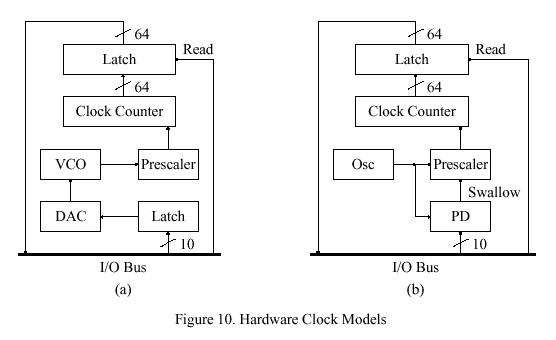
A design sketch of a computer clock constructed entirely of hardware logic components is shown in Figure 10a. The clock is read by first pulsing the read signal, which latches the current value of the clock counter, then adding the contents of the clock-counter latch and a 64-bit clock-offset variable, which is maintained in processor memory. The clock phase is adjusted by adding a correction to the clock-offset variable, while the clock frequency is adjusted by loading a correction to the DAC latch. In principle, this clock model can be adapted to any precision by changing the number of bits of the prescaler or clock counter or changing the VCO frequency. However, it does not seem useful to reduce precision much below the minimum interrupt latency, which is in the low microseconds for a modern RISC processor.
If it is not possible to vary the oscillator frequency, which might be the case if the oscillator is an external frequency standard, a design such as shown in Figure 10b may be used. It includes a fixed-frequency oscillator and prescaler which includes a dual-modulus swallow counter that can be operated in either divide-by-10 or divide-by-11 modes as controlled by a pulse produced by a programmable divider (PD). The PD is loaded with a value representing the frequency offset. Each time the divider overflows a pulse is produced which switches the swallow counter from the divide-by-10 mode to the divide-by-11 mode and then back again, which in effect "swallows" or deletes a single pulse of the prescaler pulse train.
The pulse train produced by the prescaler is controlled precisely over a small range by the contents of the PD. If programmed to emit pulses at a low rate, relatively few pulses are swallowed per second and the frequency counted is near the upper limit of its range; while, if programmed to emit pulses at a high rate, relatively many pulses are swallowed and the frequency counted is near the lower limit. Assuming some degree of freedom in the choice of oscillator frequency and prescaler ratios, this design can compensate for a wide range of oscillator frequency tolerances.
In all of the above designs it is necessary to limit the amount of adjustment incorporated in any step to insure that the system clock indications are always monotonically increasing. With the software clock model this is assured as long as the increment is never negative. When the magnitude of a phase adjustment exceeds the tick interval (as corrected for the frequency adjustment), it is necessary to spread the adjustments over multiple tick intervals. This strategy amounts to a deliberate frequency offset sustained for an interval equal to the total number of ticks required and, in fact, is a feature of the Unix clock model discussed below.
In the hardware clock models the same considerations apply; however, in these designs the tick interval amounts to a single pulse at the prescaler output, which may be in the order of 1 ms. In order to avoid decreasing the indicated time when a negative phase correction occurs, it is necessary to avoid modifying the clock-offset variable in processor memory and to confine all adjustments to the VCO or prescaler. Thus, all phase adjustments must be performed by means of programmed frequency adjustments in much the same way as with the software clock model described previously.
It is interesting to conjecture on the design of a processor assist that could provide all of the above functions in a compact, general-purpose hardware interface. The interface might consist of a multifunction timer chip such as the AMD 9513A, which includes five 16-bit counters, each with programmable load and hold registers, plus an onboard crystal oscillator, prescaler and control circuitry. A 48-bit hardware clock counter would utilize three of the 16-bit counters, while the fourth would be used as the swallow counter and the fifth as the programmable divider. With the addition of a programmable-array logic device and architecture-specific host interface, this compact design could provide all the functions necessary for a comprehensive timekeeping system.
The Fuzzball Clock Model
The Fuzzball clock model uses a combination of hardware and software to provide precision timing with a minimum of software and processor overhead. The model includes an oscillator, prescaler and hardware counter; however, the oscillator frequency remains constant and the hardware counter produces only a fraction of the total number of bits required by the clock counter. A typical design uses a 64-bit software clock counter and a 16-bit hardware counter which counts the prescaler output. A hardware-counter overflow causes the processor to increment the software counter at the bit corresponding to the frequency 2N f p, where N is the number of bits of the hardware counter and fp is the counted frequency at the prescaler output. The processor reads the clock counter by first generating a read pulse, which latches the hardware counter, and then adding its contents, suitably aligned, to the software counter.
The Fuzzball clock can be corrected in phase by adding a (signed) adjustment to the software clock counter. In practice, this is done only when the local time is substantially different from the time indicated by the clock and may violate the monotonicity requirement. Vernier phase adjustments determined in normal system operation must be limited to no more than the period of the counted frequency, which is 1 kHz for LSI-11 Fuzzballs. In the Fuzzball model these adjustments are performed at intervals of 4 s, called the adjustment interval, which provides a maximum frequency adjustment range of 250 ppm. The adjustment opportunities are created using the interval-timer facility, which is a feature of most operating systems and independent of the time-of-day clock. However, if the counted frequency is increased from 1 kHz to 1 MHz for enhanced precision, the adjustment frequency must be increased to 250 Hz, which substantially increases processor overhead. A modified design suitable for high precision clocks is presented in the next section.
In some applications involving the Fuzzball model, an external pulse-per-second (pps) signal is available from a reference source such as a cesium clock or GPS receiver. Such a signal generally provides much higher accuracy than the serial character string produced by a radio timecode receiver, typically in the low nanoseconds. In the Fuzzball model this signal is processed by an interface which produces a hardware interrupt coincident with the arrival of the pps pulse. The processor then reads the clock counter and computes the residual modulo 1 s of the clock counter. This represents the local-clock error relative to the pps signal.
Assuming the seconds numbering of the clock counter has been determined by a reliable source, such as a timecode receiver, the offset within the second is determined by the residual computed above. In the NTP local-clock model the timecode receiver or NTP establishes the time to within ±128 ms, called the aperture, which guarantees the seconds numbering to within the second. Then, the pps residual can be used directly to correct the oscillator, since the offset must be less than the aperture for a correctly operating timecode receiver and pps signal.
The above technique has an inherent error equal to the latency of the interrupt system, which in modern RISC processors is in the low tens of microseconds. It is possible to improve accuracy by latching the hardware time-of-day counter directly by the pps pulse and then reading the counter in the same way as usual. This requires additional circuitry to prioritize the pps signal relative to the pulse generated by the program to latch the counter.
The Unix Clock Model
The Unix 4.3bsd clock model is based on two system calls, settimeofday and adjtime, together with two kernel variables tick and tickadj. The settimeofday call unceremoniously resets the kernel clock to the value given, while the adjtime call slews the kernel clock to a new value numerically equal to the sum of the present time of day and the (signed) argument given in the adjtime call. In order to understand the behavior of the Unix clock as controlled by the Fuzzball clock model described above, it is helpful to explore the operations of adjtime in more detail.
The Unix clock model assumes an interrupt produced by an onboard frequency source, such as the clock counter and prescaler described previously, to deliver a pulse train in the 100-Hz range. In principle, the power grid frequency can be used, although it is much less stable than a crystal oscillator. Each interrupt causes an increment called tick to be added to the clock counter. The value of the increment is chosen so that the clock counter, plus an initial offset established by the settimeofday call, is equal to the time of day in microseconds.
The Unix clock can actually run at three different rates, one corresponding to tick, which is related to the intrinsic frequency of the particular oscillator used as the clock source, one to tick + tickadj and the third to tick -tickadj. Normally the rate corresponding to tick is used; but, if adjtime is called, the argument delta given is used to calculate an interval DELTA t = delta tick over tickadj during which one or the other of the two rates are used, depending on the sign of delta. The effect is to slew the clock to a new value at a small, constant rate, rather than incorporate the adjustment all at once, which could cause the clock to be set backward. With common values of tick = 10 ms and tickadj = 5 us, the maximum frequency adjustment range is ± tickadj over tick = +- {5 x 10⁻⁶} over {10-2} or ±500 ppm. Even larger ranges may be required in the case of some workstations (e.g., SPARC stations) with extremely poor component tolerances.
When precisions not less than about 1 ms are required, the Fuzzball clock model can be adapted to the Unix model by software simulation, as described in Section 5 of the NTP specification, and calling adjtime at each adjustment interval. When precisions substantially better than this are required, the hardware microsecond clock provided in some workstations can be used together with certain refinements of the Fuzzball and Unix clock models. The particular design described below is appropriate for a maximum oscillator frequency tolerance of 100 ppm (.01%), which can be
obtained using a relatively inexpensive quartz crystal oscillator, but is readily scalable for other assumed
tolerances.
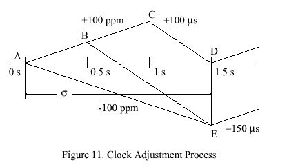
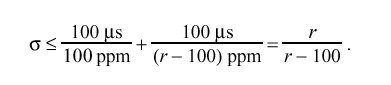
The clock model requires the capability to slew the clock frequency over the range ±100 ppm with an intrinsic oscillator frequency error as great as ±100 ppm. Figure 11 shows the timing relationships at the extremes of the requirements envelope. Starting from an assumed offset of nominal zero and an assumed error of +100 ppm at time 0 s, the line AC shows how the uncorrected offset grows with time. Let sigma represent the adjustment interval and a the interval AB, in seconds, and let r be the slew, or rate at which corrections are introduced, in ppm. For an accuracy specification of 100 us, then
The line AE represents the extreme case where the clock is to be steered -100 ppm. Since the slew must be complete at the end of the adjustment interval,
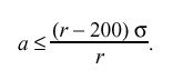
These relationships are satisfied only if r > 200 ppm and sigma < 2 s. Using r = 300 ppm for convenience, sigma = 1.5 s and a < 0.5 s. For the Unix clock model with tick = 10 ms, this results in the value of tickadj = 3us.
One of the assumptions made in the Unix clock model is that the period of adjustment computed in the adjtime call must be completed before the next call is made. If not, this results in an error message to the system log. However, in order to correct for the intrinsic frequency offset of the clock oscillator, the NTP clock model requires adjtime to be called at regular adjustment intervals of sigma s. Using the algorithms described here and the architecture constants in the NTP specification, these adjustments will always complete.
Mathematical Model of the NTP Logical Clock
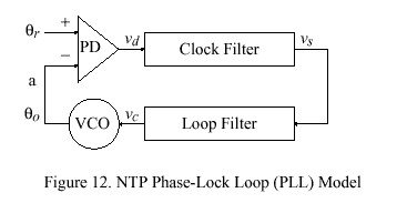
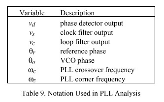
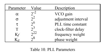
The NTP logical clock can be represented by the feedback-control model shown in Figure 12. The model consists of an adaptive-parameter, phase-lock loop (PLL), which continuously adjusts the phase and frequency of an oscillator to compensate for its intrinsic jitter, wander and drift. A mathematical analysis of this model developed along the lines of [SMI86] is presented in following sections, along with a design example useful for implementation guidance in operating-systems environments such as Unix and Fuzzball. Table 9 summarizes the quantities ordinarily treated as variables in the model. By convention, v is used for internal loop variables, theta for phase, omega for frequency and tau for time. Table 10 summarizes those quantities ordinarily fixed as constants in the model. Note that these are all expressed as a power of two in order to simplify the implementation.
In Figure 12 the variable theta sub r represents the phase of the reference signal and theta sub o the phase of the voltage-controlled oscillator (VCO). The phase detector (PD) produces a voltage v sub d representing the phase difference theta sub r - theta sub o . The clock filter functions as a tapped delay line, with the output v sub s taken at the tap selected by the clock-filter algorithm described in the NTP specification. The loop filter, represented by the equations given below, produces a VCO correction voltage v sub c, which controls the oscillator frequency and thus the phase theta sub o.
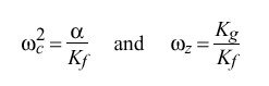
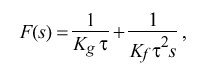
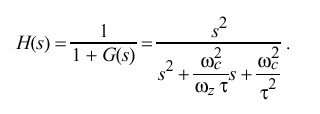
The PLL behavior is completely determined by its open-loop, Laplace transfer function G(s) in the s domain. Since both frequency and phase corrections are required, an appropriate design consists of a type-II PLL, which is defined by the function
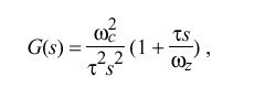
where omega sub c is the crossover frequency (also called loop gain), omega sub z is the corner frequency (required for loop stability) and tau determines the PLL time constant and thus the bandwidth. While this is a first-order function and some improvement in phase noise might be gained from a higher-order function, in practice the improvement is lost due to the effects of the clock-filter delay, as described below.
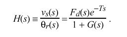
The open-loop transfer function G(s) is constructed by breaking the loop at point a on Figure 12 and computing the ratio of the output phase theta sub o (s) to the reference phase theta sub r (s). This function is the product of the individual transfer functions for the phase detector, clock filter, loop filter and VCO. The phase detector delivers a voltage v sub d (t) = theta sub r (t), so its transfer function is simply F sub d (s) = 1, expressed in V/rad. The VCO delivers a frequency change DELTA omega = { d theta sub o (t)} over {dt} = alpha {v sub c (t)}, where alpha is the VCO gain in rad/V-sec and theta sub o (t) = alpha int v sub c (t) dt. Its transfer function is the Laplace transform of the integral, F sub o (s) = alpha over s, expressed in rad/V. The clock filter contributes a stochastic delay due to the clock-filter algorithm; but, for present purposes, this delay will be assumed a constant T, so its transfer function is the Laplace transform of the delay, F sub s (s) = e sup {- Ts}. Let F(s) be the transfer function of the loop filter, which has yet to be determined. The open-loop transfer function G(s) is the product of these four individual transfer functions:
For the moment, assume that the product Ts is small, so that e sup {-Ts} approx 1. Making the following substitutions,
and rearranging yields
which corresponds to a constant term plus an integrating term scaled by the PLL time constant tau. This form is convenient for implementation as a sampled-data system, as described later.
With the parameter values given in Table 10, the Bode plot of the open-loop transfer function G(s) consists of a -12 dB/octave line which intersects the 0-dB baseline at omega sub c = 2 sup -12 rad/s, together with a +6 dB/octave line at the corner frequency omega sub z = 2 sup -14 rad/s. The damping factor zeta = omega sub c over {2 omega sub z} = 2 suggests the PLL will be stable and have a large phase margin together with a low overshoot. However, if the clock-filter delay T is not small compared to the loop delay, which is approximately equal to 1 over omega sub c, the above analysis becomes unreliable and the loop can become unstable. With the values determined as above, T is ordinarily small enough to be neglected.
Assuming the output is taken at v sub s, the closed-loop transfer function H(s) is
If only the relative response is needed and the clock-filter delay can be neglected, H(s) can be written
For some input function I(s) the output function I(s)H(s) can be inverted to find the time response. Using a unit-step input I(s) = 1 over s and the values determined as above, This yields a PLL rise time of about 52 minutes, a maximum overshoot of about 4.8 percent in about 1.7 hours and a settling time to within one percent of the initial offset in about 8.7 hours.
Parameter Management
A very important feature of the NTP PLL design is the ability to adapt its behavior to match the prevailing stability of the local oscillator and transmission conditions in the network. This is done using the <$Ealpha> and <$Etau> parameters shown in Table 10. Mechanisms for doing this are described in following sections.
Adjusting VCO Gain
The alpha parameter is determined by the maximum frequency tolerance of the local oscillator and the maximum jitter requirements of the timekeeping system. This parameter is usually an architecture constant and fixed during system operation. In the implementation model described below, the reciprocal of alpha, called the adjustment interval sigma, determines the time between corrections of the local clock, and thus the value of alpha. The value of sigma can be determined by the following procedure.
The maximum frequency tolerance for board-mounted, uncompensated quartz-crystal oscillators is probably in the range of 10-4 (100 ppm). Many if not most Internet timekeeping systems can tolerate jitter to at least the order of the intrinsic local-clock resolution, called precision in the NTP specification, which is commonly in the range from one to 20 ms. Assuming 10-3 s peak-to-peak as the most demanding case, the interval between clock corrections must be no more than sigma = 10 sup -3 over {2 x 10 sup -4} = 5 sec. For the NTP reference model sigma = 4 sec in order to allow for known features of the Unix operating-system kernel. However, in order to support future anticipated improvements in accuracy possible with faster workstations, it may be useful to decrease sigma to as little as one-tenth the present value.
Note that if sigma is changed, it is necessary to adjust the parameters K sub f and K sub g in order to retain the same loop bandwidth; in particular, the same omega sub c and omega sub z. Since alpha varies as the reciprocal of sigma, if sigma is changed to something other than 22, as in Table 10, it is necessary to divide both K sub f and K sub g by sigma over 4 to obtain the new values.
Adjusting PLL Bandwidth
A key feature of the type-II PLL design is its capability to compensate for the intrinsic frequency errors of the local oscillator. This requires a initial period of adaptation in order to refine the frequency estimate (see later sections of this appendix). The tau parameter determines the PLL time constant and thus the loop bandwidth, which is approximately equal to {omega sub c} over tau. When operated with a relatively large bandwidth small tau, as in the analysis above, the PLL adapts quickly to changes in the input reference signal, but has poor long term stability. Thus, it is possible to accumulate substantial errors if the system is deprived of the reference signal for an extended period. When operated with a relatively small bandwidth large tau, the PLL adapts slowly to changes in the input reference signal, and may even fail to lock onto it. Assuming the frequency estimate has stabilized, it is possible for the PLL to coast for an extended period without external corrections and without accumulating significant error.
In order to achieve the best performance without requiring individual tailoring of the loop bandwidth, it is necessary to compute each value of tau based on the measured values of offset, delay and dispersion, as produced by the NTP protocol itself. The traditional way of doing this in precision timekeeping systems based on cesium clocks, is to relate tau to the Allan variance, which is defined
as the mean of the first-order differences of sequential samples measured during a specified interval tau,
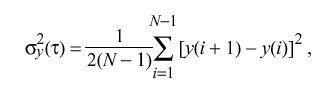
where y is the fractional frequency measured with respect to the local time scale and N is the number of samples.
In the NTP local-clock model the Allan variance (called the compliance, h in Table 11) is approximated on a continuous basis by exponentially averaging the first-order differences of the offset samples using an empirically determined averaging constant. Using somewhat ad-hoc mapping functions determined from simulation and experience, the compliance is manipulated to produce the loop time constant and update interval.
The NTP Clock Model
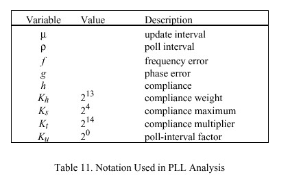
The PLL behavior can also be described by a set of recurrence equations, which depend upon several variables and constants. The variables and parameters used in these equations are shown in Tables 9, 10 and 11. Note the use of powers of two, which facilitates implementation using arithmetic shifts and avoids the requirement for a multiply/divide capability.
A capsule overview of the design may be helpful in understanding how it operates. The logical clock is continuously adjusted in small increments at fixed intervals of sigma. The increments are determined while updating the variables shown in Tables 9 and 11, which are computed from received NTP messages as described in the NTP specification. Updates computed from these messages occur at discrete times as each is received. The intervals mu between updates are variable and can range up to about 17 minutes. As part of update processing the compliance h is computed and used to adjust the PLL time constant tau. Finally, the update interval rho for transmitted NTP messages is determined as a fixed multiple of tau.
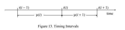
Updates are numbered from zero, with those in the neighborhood of the ith update shown in Figure 13. All variables are initialized at i = 0 to zero, except the time constant tau (0) = tau, poll interval mu (0) = tau (from Table 10) and compliance h (0) = K sub s. After an interval mu (i)> ( i > 0) from the previous update the ith update arrives at time t(i) including the time offset v sub s (i). Then, after an interval mu (i +1) the i+1th update arrives at time t(i + 1) including the time offset v sub s (i + 1). When the update v sub s (i) is received, the frequency error f(i + 1) and phase error g(i+1) are computed:
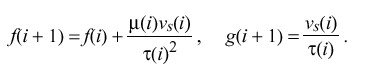
Note that these computations depend on the value of the time constant tau (i)> and poll interval mu (i) previously computed from the i-1th update. Then, the time constant for the next interval is computed from the current value of the compliance h(i)
![]()
Next, using the new value of tau, called tau prime to avoid confusion, the poll interval is computed
![]()
Finally, the compliance h(i + 1) is recomputed for use in the i+1th update:
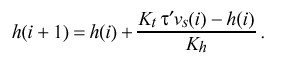
The factor tau prime in the above has the effect of adjusting the bandwidth of the PLL as a function of compliance. When the compliance has been low over some relatively long period, tau prime is increased and the bandwidth is decreased. In this mode small timing fluctuations due to jitter in the network are suppressed and the PLL attains the most accurate frequency estimate. On the other hand, if the compliance becomes high due to greatly increased jitter or a systematic frequency offset, tau prime is decreased and the bandwidth is increased. In this mode the PLL is most adaptive to transients which can occur due to reboot of the system or a major timing error. In order to maintain optimum stability, the poll interval rho is varied directly with tau.
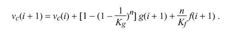
A model suitable for simulation and parameter refinement can be constructed from the above recurrence relations. It is convenient to set the temporary variable a = g(i +1). At each adjustment interval sigma the quantity a over K sub g + {f(i + 1)} over K sub f is added to the local-clock phase and the quantity a over K sub g is subtracted from a. For convenience, let n be the greatest integer in {mu (i)} over sigma; that is, the number of adjustments that occur in the ith interval. Thus, at the end of the ith interval just before the i+1th update, the VCO control voltage is:
Detailed simulation of the NTP PLL with the values specified in Tables 9, 10 and 11 and the clock filter described in the NTP specification results in the following characteristics: For a 100-ms phase change the loop reaches zero error in 39 minutes, overshoots 7 ms at 54 minutes and settles to less than 1 ms in about six hours. For a 50-ppm frequency change the loop reaches 1 ppm in about 16 hours and 0.1 ppm in about 26 hours. When the magnitude of correction exceeds a few milliseconds or a few ppm for more than a few updates, the compliance begins to increase, which causes the loop time constant and update interval to decrease. When the magnitude of correction falls below about 0.1 ppm for a few hours, the compliance begins to decrease, which causes the loop time constant and update interval to increase. The effect is to provide a broad capture range exceeding 4 s per day, yet the capability to resolve oscillator skew well below 1 ms per day. These characteristics are appropriate for typical crystal-controlled oscillators with or without temperature compensation or oven control.